Highly versatile
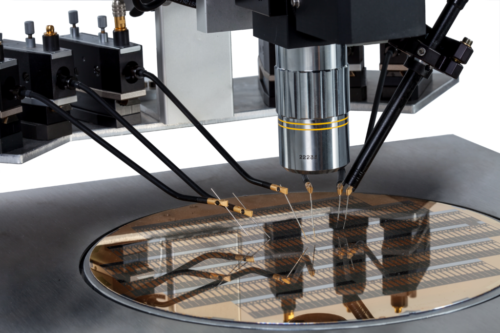
The system allows you to assess large and small-signal material properties all these materials and components across a broad temperature range. Our range of high-voltage amplifiers is sure to have the right solution for your individual needs for electrical excitation. The entire system, including the amplifiers, is controlled by our aixPlorer3.0 software. You can then measure the sample’s current response with Virtual Ground current amplifiers. Alongside this, you can record other measurements like the sample displacement. Our aixLook software not only visualizes the camera images, but is also used to control the positioning tables.
Intuitive operation
We love finding solutions, which is why we are dedicated to full system integration on existing probing systems. Our Automation Assistant controls the increasingly sophisticated systems, and is set to do the same for the aixSCAN tools in future. As a user, you benefit from the redesigned GUI, enabling intuitive and easy operation. You can use our ScanningPES system in the following applications:
-
WHAT YOU CAN DO
- Electrical polarization and displacement measurements with large-signal excitation (uni and bipolar)
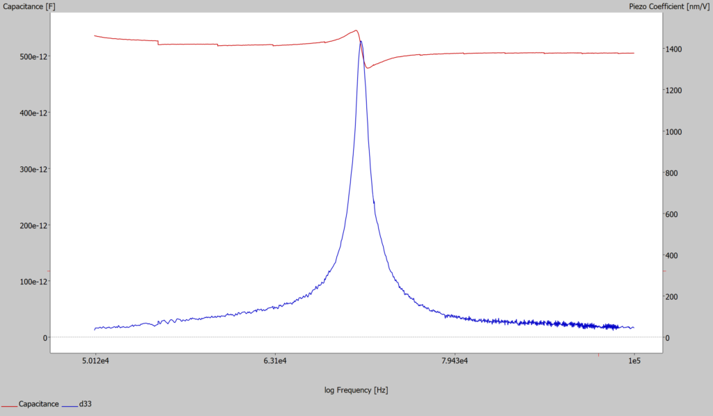
- Small signal capacitance, loss factor and piezo coefficient via uni and bipolar DC voltage
- Temperature-based studies of electrical and electromechanical properties
- Pyroelectric measurements
- Leakage current measurements
- Lifetime tests
- Impedance measurements
- User-defined excitation signals
-
THE BENEFITS FOR YOU
- One system for comprehensive assessment of piezo and ferroelectric thin and thick films, MEMS structures, bulk materials, sensor and actuator systems
- One piece of software for external hardware control (e.g. temperature controller, high-voltage amplifier, travel sensor, impedance analyzer, oscilloscope) and data collection
- Automated variants with up to 8-inch heating systems for temperature-based measurements
- Laser interferometer with spot size sizes with a minimum diameter ranging to 5 µm
- Camera with microscope lenses
- Remote access and script control available
- Recipe editor and wafer mapping
- Optional database connection (ODBC) for easy access to material and device properties
- User support
-
WHAT THIS MEANS FOR YOU
- Fast, automated measurement of a range of samples -> get a high-quality statistical database quicker, e.g. for aging estimations
- Systems are flexible and easy to adapt to your specific requirements
- Measurement support throughout the entire development and production phases
- Highly precise and repeatable measurements for process-sensitive determination of relevant parameters
- Shorter time to market